Lab 15 Faculty-designed Board measurements
Practical PCB Design and Manufacture- Lab 15 Report
Faculty-designed Board 2 Measurements
Quinton Corry - quco3046@colorado.edu
Introduction
Recently, we designed a PCB to illustrate the good and bad design practices to use and not use, unless we can give a strong compelling reason otherwise. This board consisted of a 555 timer output connected to two different hex inverter circuits, with one of these circuits demonstrating good design practices, and the other demonstrating bad design practices. Before we received the boards that we designed to bring up, assemble, and test, we were able to take measurements from an almost identical board that was designed by a faculty member. From this lab, we were able to gain a good understanding of what to look for and measure when we got our boards back.
Tools and Components
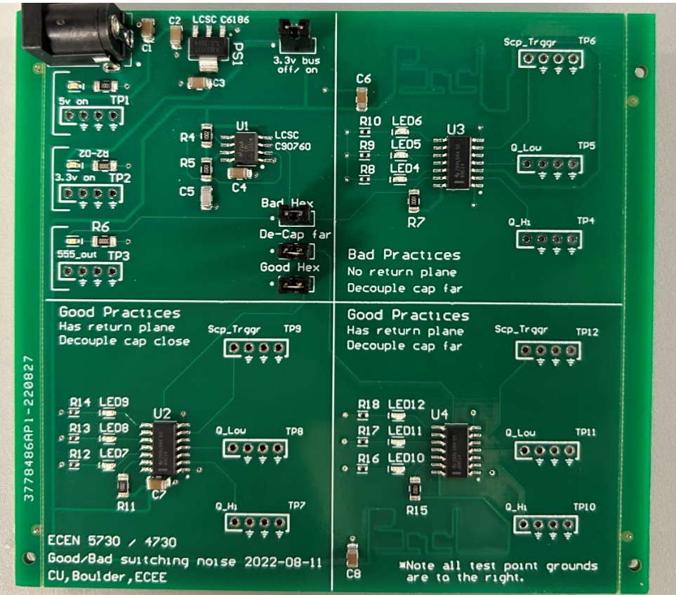
Figure 1.) Hex inverter board with three different regions for showing good/bad design practices. The “good” region (bottom left) uses a ground plane, separate return paths, and a decoupling capacitor that is close to the hex inverter IC. The “better” region (bottom right) uses a ground plane, separate return paths, and a decoupling capacitor that is far away from the hex inverter IC. The “bad” region (top right) does not use a ground plane, has shared return paths, and a decoupling capacitor that is far away from the hex inverter IC.
The regions will be referred to as “good,” “better,” and “bad” for the remainder of this document as referenced in Figure 1.
Measurements
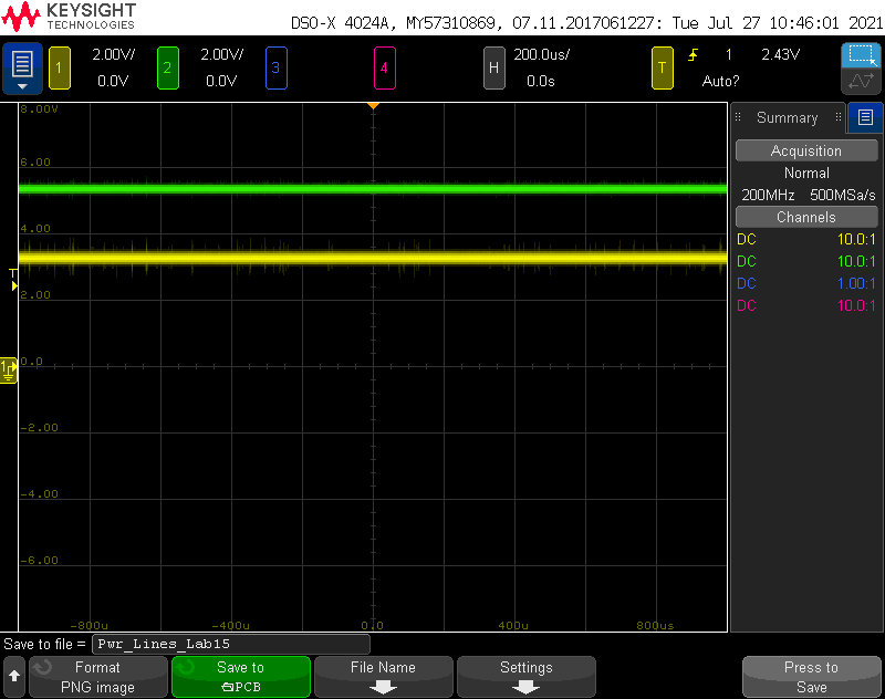
I first ensured that both the 5V and 3.3V power lines were at the indicated voltages:
Figure 2.) Channel 1 (yellow) is measuring the 3.3V power line and channel 2 (green) is measuring the 5V power line with both channels at 2V/div and the time scale at 200us/div. The 3.3V power line is around 3.3V and the 5V power line is slightly higher than 5V
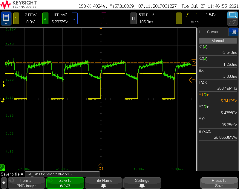
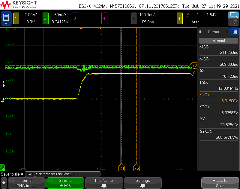
The switching noise on both power lines is pictured below:
Figure 3a.) Channel 1 (yellow) has a scale of 2V/div and channel 2 Figure 3b.) Channel 1 (yellow) has a scale of 2V/div and
(green)has a scale of 50mV/div with an offset of 3.24V. The horizontal channel 2 (green) has a scale of 100mV/div with an offset
scale is 100ns/div. Switching noise on the 3.3V line (green) with of 5.234V. The horizontal scale is 500us/div. Total
the scope triggered on the 555 output (yellow) which has a rise time switching noise on the 5V line (green) is about 100mV
of approximately 50ns with the scope triggering on the 555 output (yellow)
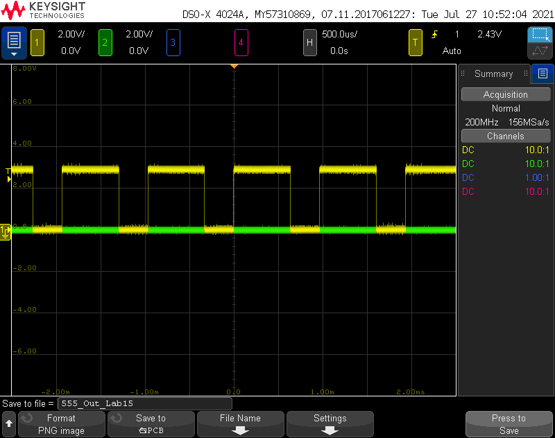
I then measured additional output parameters of the 555 output:
Figure 4.) Channel 1 (yellow) is measuring 555 output with the vertical scale at 2V/div and the time scale at 500us/div. The 555 has a duty cycle of about 60% and a period of 1 ms
Next I took measurements of the quiet low and quiet high pins (denoted as Q_low and Q_high on the board in figure 1) in each region of the board.
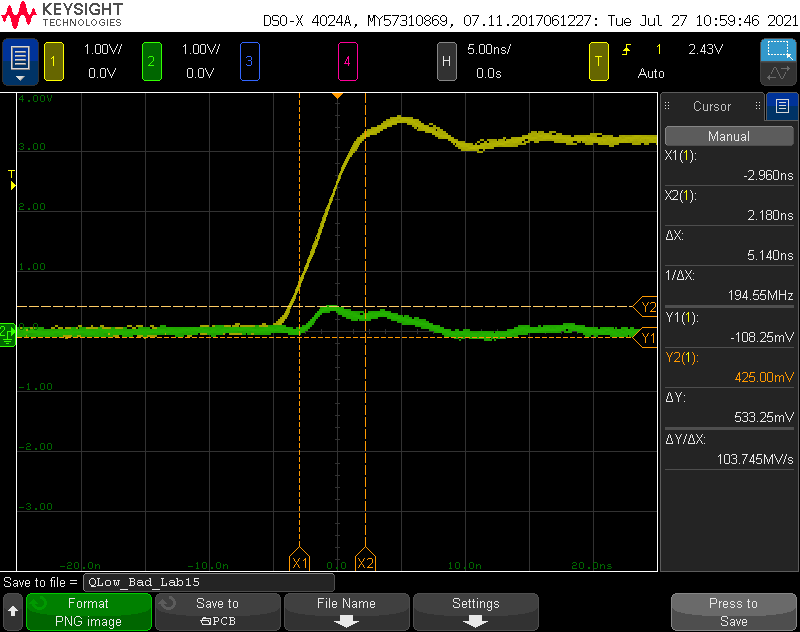
Bad Region Measurements:
Figure 5.) Channel 1 (yellow) is measuring a hex inverter output indicated by “Scp_trggr” on the board and channel two (green) is measuring the quiet low pin. The vertical scale is at 1V/div and the time scale at 5ns/div.
The quiet low noise is about 0.5V and the rise time of the trigger signal is approximately 5ns. This rise time is much shorter than the 555 rise time.
Figure 6.) Channel 1 (yellow) is measuring a hex inverter output indicated by “Scp_trggr” on the board and channel two (green) is measuring the quiet high pin. Channel one has an offset of 12.5 mv and channel two has an offset of 912.5 mV. The vertical scale is at 1V/div and the time scale at 5ns/div.
The quiet high noise is about 1V. The relatively high amount of noise on the quiet pins likely originates from the shared return paths, far away decoupling capacitor, and lack of a ground plane within the region of the board.
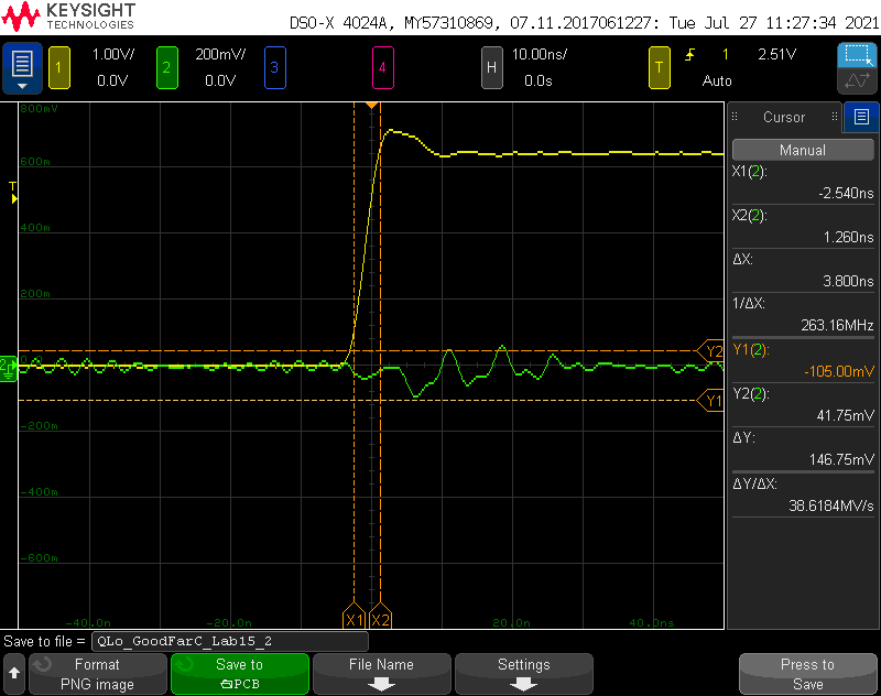
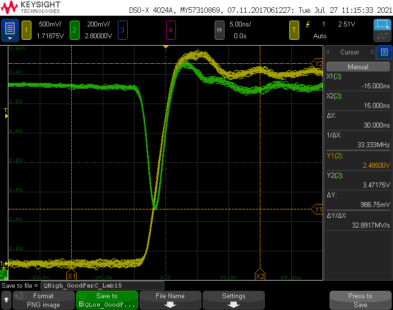
Better Region Measurements:
Figure 7.) Channel 1 (yellow) is measuring a hex inverter output indicated by “Scp_trggr” on the board and channel two (green) is measuring the quiet low pin. Channel 1 has a vertical scale at 1V/div, channel 2 has a vertical scale of 200mV/div, and the time scale at 10ns/div.
The quiet low noise is about 150mV and the rise time of the trigger signal is approximately 4ns.
Figure 8.) Channel 1 (yellow) is measuring a hex inverter output indicated by “Scp_trggr” on the board and channel two (green) is measuring the quiet high pin. Channel 1 has a vertical scale at 500mV/div with an offset of about 1.7V, channel 2 has a vertical scale of 200mV/div with an offset of 2.8V, and the time scale at 5ns/div.
The quiet high noise is still about 1V. This is likely due to the fact that the decoupling capacitor is still far away from the hex inverter IC, resulting in a high amount of loop inductance. While a ground plane and separate return paths reduce noise on the quiet low pin, there is still a considerable amount of noise on the quiet high pin.
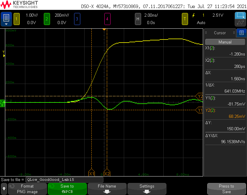
Good Region Measurements:
Figure 9.) Channel 1 (yellow) is measuring a hex inverter output indicated by “Scp_trggr” on the board and channel two (green) is measuring the quiet low pin. Channel 1 has a vertical scale at 1V/div, channel 2 has a vertical scale of 200mV/div, and the time scale at 2ns/div.
The quiet low noise is about the same as the “better” region’s quiet low noise at 150mV and the rise time of the trigger signal is approximately 2ns. The similarity in noise is likely due to the fact that the only difference between the “good” and “better” regions is the proximity of the decoupling capacitor and the hex inverter IC, with the “good” region having a closer decoupling capacitor.
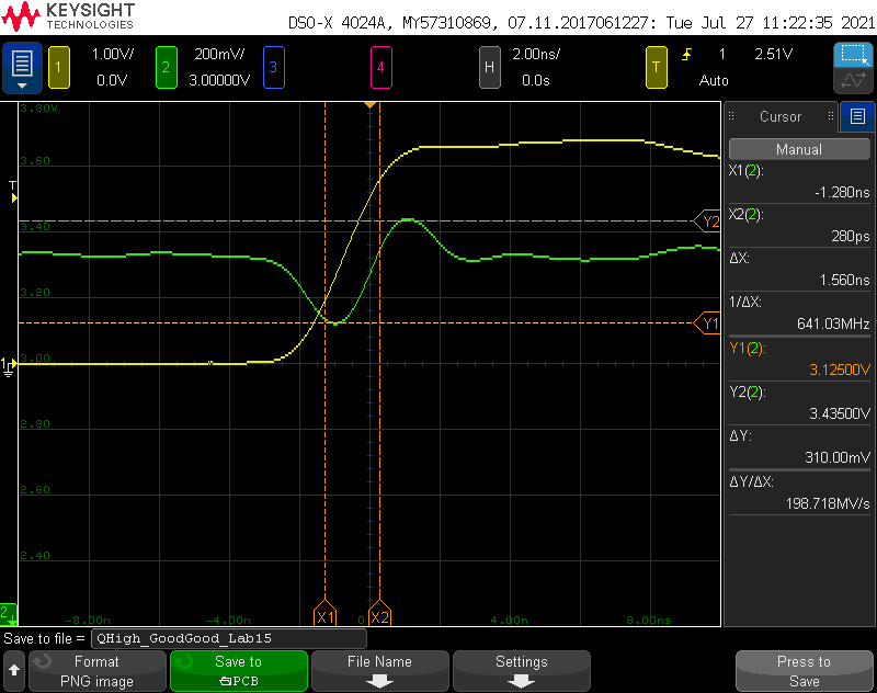
Figure 10.) Channel 1 (yellow) is measuring a hex inverter output indicated by “Scp_trggr” on the board and channel two (green) is measuring the quiet high pin. Channel 1 has a vertical scale at 1V/div with, channel 2 has a vertical scale of 200mV/div with an offset of 3V, and the time scale at 2ns/div.
The quiet high noise for this region has decreased by about 66% to 300mV, since the decoupling capacitor is much closer to the hex inverter IC.
Takeaways